ENGR210
Project 6: Arithmetic Logic Unit
Due: Wednesday March 11th
Overview
You will design and implement an 8-bit Arithmetic Logic Unit (ALU). You can use the same design procedure to expand to a functionally complete 16-, or 32-bit ALU. You will also get to implement a basic D Flip-Flop. Flip Flops are used to add state to your digital systems.
Background
Arrays
For the last project, we expressed the d outputs of the decoder seperately:
module decoder (
    input a, b, c,
    output d0, d1, d2, d3, d4, d5, d6, d7
    );
However it is also possible to combine them into a single array of wires:
module decoder (
    input a, b, c,
    output [7:0] d
    );
Note that the array definition is of the form:
type [mostSignificantIndex:leastSignificantIndex] name;
Thus, the big index goes on the left, and the smaller index (typically 0) on the right, It is possible to create arrays differeing from this convention, but we do not recommend it.
Individual wires can be accessed with the standard array syntax “[ ]” that you’ve seen from C or Python:
assign d[1] = ~a && ~b && c;
wire wire1 = d[0] ^ d[1];
You can also access groups of bits from within an array using the colon slicing similar to Python. For example, this will access bits 5, 4, and 3 from d and assign them to bits 2, 1, and 0 of other_wire2.
wire [2:0] wire2 = d[5:3];
A few other useful array operations are concatenation and static assignment. Concatenation lets you join multiple signals together to create an array using curly-brackets. The following example joins three wires (a, b, and c) to make a 3-wire array wire3.
wire [2:0] wire3 = { a, b, c }; //concatenation
Static assignment lets you fix a wire to a given logical value, for example 1. The 'h prefix is Verilog’s method of specifing hexadecima. Recal that C and Python 3 use the “0x” prefix. You can also use 'b to specify a binary number.
    wire wire4 = 'h0; // static assignment
    wire [2:0] wire5 = 'b010; // also static assignment
    wire [2:0] wire6 = { 'b0, 'b1, 'b0 }; // static + concatenation
Sometimes it’s helpful to specify the number of bits for a number. You can do this by placing the number of bits for a number ahead of the 'h. In the following example, we specify that the first number is two bits wide, and the second number is only 1 bit wide.
wire [2:0] wire6 = { 2'b1, 1'b0 }; // binary 01 & 1
Case Statements
Another piece of new Verilog for this lab is the case statement. Just like C, verilog lets you use case statements. The syntax looks something like this:
case(sel)

    2`b00: out = input[0]; // set out = input[0] when sel == 00
    2`b01: out = input[1]; // set out = input[1] when sel == 01
    2`b10: out = input[2]; // set out = input[2] when sel == 10
    2`b11: out = input[3]; // set out = input[3] when sel == 11
    default: out = input[0]; // you usualy want a default case

endcase
Combinational Always Blocks
Unfortunately, you cannot use case statements with assign, it must be inside a special block called always_comb. The comb is short for combinational. always_comb blocks look like this:
always_comb begin
    out = input[2];
end
always_comb blocks run all of the commands between begin//end every time something on the right-hand side of any contained equation changes. In the above block, the right-hand-side is shown in bold. That means whenever anything changes, verilog wil re-evaluate all the block’s assignments. The above block is functionally equivalent to assign out = input[2];
As Verilog is an odd language, and you cannot assign a value to a 'wire' inside an always block. Therefor we declare out as a logic type. There are subtle differences between wire and logic, but for now just remember that everything inside an always block must be declared logic.
If we put the always block and the case statement together, we get something that looks like this:
logic out; //must be logic (or reg) for always blocks

always_comb begin

    out = 1'h0; //default
    case(sel)

        2`b00: out = input[0];
        2`b01: out = input[1];
        2`b10: out = input[2];
        2`b11: out = input[3];

    endcase
end
This lets us set out to one of 4 values based on the value of sel (or select). This is one way to build a 4-1 multiplexer.
Flip-Flop Always Blocks
One final piece is how to build D Flip Flops in Verilog. Here again we make use of an always block, but this one looks a little different.
wire clk, D;  //input signals
logic Q, Qbar;//must be logic (or reg) for always blocks

//D Flip Flop

always_ff @ (posedge clk)
begin
    Q    <=  D;
    Qbar <= ~D; //optional

end
Notice this always block is an always_ff, “ff” is short for “flip-flop”. It also includes @(posedge clk) or “at the positive edge of clock”. This means only the positive (rising) edge of clk will cause signals inside the always block to chane. A positive edge is when a signal which was 0 (a low voltage) rises to 1 (a high voltage). Thus, there is a “positive” or “rising” edge in the waveform. Unless clk is rising (going from 0 to 1), none of the outputs will change. This is what makes this block into a flip flop. As Q and Qbar can hold state, they must be declared as logic or the older reg. Also notice the use of the non-blocking assignment (<=). We will discuss this more in class, but the rule is:
always_comb is for combinational logic and ONLY USES BLOCKING ASSIGNMENTS (=)
always_ff @(posedge ...) is for sequential logic and ONLY USES NON-BLOCKING ASSIGNMENTS (<=)
DEBUGGING PAIN WILL RESULT IF YOU BREAK THE ABOVE RULE!!
Verilog being an odd language, the tools will not check for this, and are more than happy to let you do whatever you want. Then you won’t understand why your FPGA does not behave as you expected. If you get a warning that says “inferring latch”, you broke the rule!
There are several other always blocks in Verilog. For now, don’t use them.
Flip-Flop Always Blocks with Enable
The previous flip-flop block always updated its state on every rising edge of clk. However, often you want to control that slightly, so that it only updates the value when you enable it. For that, we add a little more logic to the always_ff block:
wire clk, D;    //input signals
**wire e;       //enable input**
logic Q, Qbar;  //must be logic (or reg) to retain state

//D Flip Flop
always_ff @(posedge clk)
begin
    **if (e) begin //only update if enabled**
        Q    <=  D;
        Qbar <= ~D; //optional
    end
end
ALU
You will build an ALU that takes two inputs; a and b, and produces three outputs: r, c, and v. Additionally, another input s will select which type of operation should be performed. Your ALU will be capable of both Arithmetic and Logical operations.
Arithmetic
Your ALU should be capable of both addition and subtraciton. We’ll assume you’ve seen digital addition before. Subtraction in the digital world can be implemented using addition and 2’s complement.
\[r = a - b = a + \bar{b} + 1\]Thus, by inverting b and adding 1, we can implement subraction. Now that we are also doing subtraction, we have chosen to express the result as r rather that s for sum.
There are a number of different ways to build adders. In practice, it is typically easiest to use the built-in Verilog addition operator (+) or subtraction operator (-) and let the tools figure it out. Unfortunately, Verilog’s built-in addition operator, by devault, assumes an 8-bit addition and results in an 8-bit sum. However, we want the carry-out, so we need a 9-bit sum. ::The solution is to prepend a 1-bit 0 to your 8-bit value to form a 9-bit value. We can use the concatenation operator in Verilog to achieve this.::
wire [7:0] a = 8`hff;
wire [8:0] a9 = {1`h0, a}; //concatenation of inputs

wire [7:0] r;
wire r9;
{r9 ,r} = a9; //concatenation of outputs
Notice for a9 we’re mashing the wire declaration and the assign-ment statement together into a single line.
In addition, your ALU should be capable of several other helpful functions
Transfer: \(r = a\)
Test: \(r = (a == 0)\)
Logic
Your ALU should also be capable of 4 basic bitwise logic operations, AND, OR, NOT, and XOR. These are computed to all bits of a and b.
Operation Encoding
To select which operand your ALU should perform, you will need to read in a 4-bit “operation select” value (here named s). The mapping of s values to operations is given below:
| s | Operation | Result |
|---|---|---|
| 1110 | AND | \(r = a \land b\) |
| 1101 | OR | \(r = a | b\) |
| 1100 | NOT | \(r = \bar{a}\) |
| 1011 | XOR | \(r = a \oplus b\) |
| 1010 | Addition | \(r = a + b\) |
| 1001 | Subtraction | \(r = a - b\) |
| 1000 | Transfer | \(r = a\) |
| 0111 | Test | \(r = (a == 0)\) |
Carry
Recall that 8-bit unsigned addition can result in a 9-it sum. Therefore, the highest bit shoulde be returned in the c bit, short for Carry. this bit must be 0 for transfer, test, and all logic operations.
Overflow
Additionally, signed arithmetic can result in overvlows. This can occur when ading two positive numbers, and receiving a negative result. Or when adding two negative numbers resulting in a positive number. This overflow condition should be captured in a v bit, short for oVerflow. ::This bit must be correct for addition and subtraction and is undefined for all other operations. If a signal is undefined, you can set it to whatever you want.::
:: SP’21 The autograder now sets c and v to 0 for all operations other than Addition or Subtraction ::
There are two ways to calculate overflow. The one discussed in class is using an XOR gate between the carry-out and the last internal carry bit of the addition/subtraction. For an 8-bit addition, this would be \(v = c_{out} \oplus c_{7}\). Unfortunately, if you use the Verilog subtraction operator (-), you will not have a \(c_{7}\).
The second way is to look at both the inputs and the result. If you construct a truth table for a[7], b[7], c[7], cout, and r(esult), it will look something like this
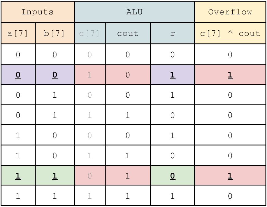
Recall the v = c[7] ^ cout. Which means it is true whenever c[7] and cout differ. Notice, there are two cases above where c[7] and cout differ, highlighted in red above. Those two cases are shown in red above. The first case occurs when a[7] == 0, b[7] == 0, and result[7] == 1. This occurs when we are adding two positive numbers, and the result is negative. The second case occurs when a[7] == 1, b[7] == 1 and result[7] == 0. Now we are adding two negative numbers and getting a positive result. We can write a Verilog expression to capture these two cases:
wire oVerflowAdd = ~a[7] & ~b[7] & r[7] | a[7] & b[7] & ~r[7];
Recall with subraction that \(A - B = A + \bar{B} + 1\). Therefor, Verilog will flip the bits of b to form ~b. It will then perform (count, result[7]) = a[7] + ~b[7] + c[7]. As part of the project, you will need to compute a similar overflow eqution for subtraction:
wire oVerflowSubtract = ??? ;
Hint: the solution can be found in the textbook
Assignment Description
8-Bit ALU
Create a Verilog file named alu.sv which defines a module as follows:
module alu(
    input        [7:0] a, //operand
    input        [7:0] b, //operand
    input        [3:0] s, //operation Select

    output logic [7:0] r, //the Result value
    output logic       c, //for unsigned Carry
    output logic       v //for signed oVerflow
);
The logic keyword is optional and can be omitted.
Your task is to implement the ALU as per the specifications above
Top-Level
Please use the following top.sv:
`timescale 1ns / 1ps

module top(
    input           CLK100MHZ,
    input   [15:0]  sw,    //operands a, b, s
    input           btnC,  //
    output  [15:0]  LED   //results c, v
);

    logic [7:0] a;

    always_ff @(posedge CLK100MHZ) begin
        if (btnC)
            a <= sw[7:0];
    end

    alu alu0(
    .a(a),
    .b(sw[7:0]),
    .s(sw[11:8]),
    .r(LED[7:0]),
    .c(LED[8]),
    .v(LED[9])
    );

    assign LED[15:12] = 5'b0;

endmodule
This module includes an 8-bit value that stores the value of a in flip flops.
logic [7:0] a; //a state-holding register for a
This module incorperates flip-flops that capture sw[7:0] and stores it to a[7:0] when the btnC button is pressed. This will capture the first input (a) for the ALU and store it, allowing you to reset sw[7:0] for the second input to the ALU (b).
You will then need to reconfigure sw[7:0] for the second input, and set the select inputs to perform the apropriate ALU operation.
As some of the LED values are unused, we assign them to 0 (off).
Remember to select “System Verilog” from the “File Type” drop-down menu.
Testbench
For this project, you only need to create a testbench for your ALU. It should be named alu\_tb.sv.
Remember to select “System Verilog” from the “File Type” drop-down menu.
MAKE SURE YOU HAVE “$display(“@@@Passed”);” AT THE END OF YOUR TESTBENCH! AND $fatal IN THE APPROPRIATE SPOT! Otherwise some bugs may not pass!
Constraints
We recommend you copy the default constraints file from here:
You will also need to reconfigure your file to align with the top-level module declaration. The names should line up properly by default.
Evaluation
The evaluation will have two steps; first,the submission of your source code and testbench to the autograder. Second, you will need t osynthesize your design, download it to the FPGA and do a demonstration for the TA.
Autograder (70%)
Log onto to https://autograder.luddy.indiana.edu and submit your code as per previous projects.
You should submit:
alu.svalu_tb.svtop.sv
Demonstration (30%)
Program your FPGA with your ALU, and demonstrate your working system to the TA. You will not recive full points until the TA has approved your demonstration.